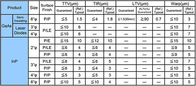
その他仕様
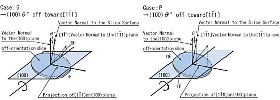
Flatness・Light Point Defects / Categories of Off-Orientation
 194KB)
Flatness
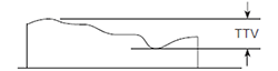
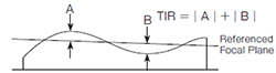
Definitions of Flatness
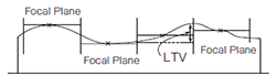
| TTV | Total Thickness Variation: The difference between the highest and the lowest elevation of the top surface of a clamped wafer. The back surface referenced. |
 |
|---|---|---|
| TIR | Total Indicated Reading: The difference between the highest point above and the lowest point below the front surface referenced focal plane of a clamped wafer. 3 points on the front surface generally used. |
 |
| LTV | Local Thickness Variation: The difference between the highest point and the lowest point within a site of the top surface of a clamped wafer. The back surface referenced. |
 |
| PLTV | Percent LTV: Percentage of sites on a wafer within the specified LTV value. |
|
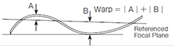
| Warp | The difference between the highest point above and the lowest point below the front surface referenced focal plane of an unclamped wafer. A least square fit on the front surface generally used. |
 |
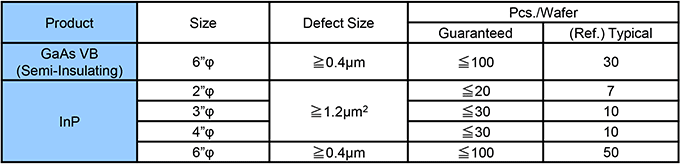
Light Point Defects
Clockwise (EJ) / Counter Clockwise (US)
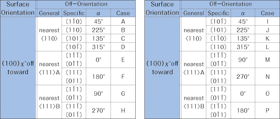
Planar Representation of Cubic Form
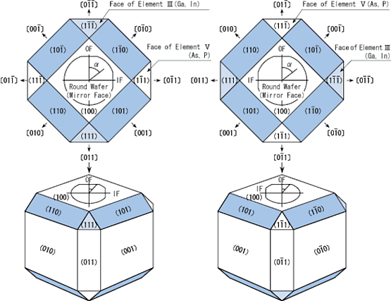
Example of off-orientation